Saturday, November 12, 2011

Shift/Jump control board finished!

After a long hiatus, I finally got the last bits of wiring finished on the Shift/Jump unit control board.  I haven't actually powered it up yet to see if it works (even if I did, I wouldn't know for sure, since I still don't have a reasonable way to get a signal onto the A/B buses).  But at least it's all wired up and ready for the (comparatively simple) transfer boards, which move a 16-bit signal from one bus to another.

Front of the control board

Yay point-to-point wiring!

Installed in the Shift/Jump unit backplane

Monday, September 26, 2011

Nice guide to 74LS vs 74HC vs 74HCT

I've been tinkering recently with my Launchpad, with the goal of developing a 32-bit I/O expander that I can use to simulate traffic on my CPU's buses without having to run an actual program.  This will allow me to debug individual modules without having to wire up the entire system, upload test software into the EEPROMs, and trace the signals across a half dozen boards.

Along the way I've had to start taking a hard look at signal voltages for various stuff, because the TI MSP430 is a 3.6V part, and I need to drive my 5V TTL and CMOS logic with it.  This requires some logic level conversion, and as it turns out, some deeper knowledge about the differences in the chips I'm plugging into my breadboard.

I was under the mistaken impression that 74LS (TTL) logic was effectively identical to 74HC (CMOS) logic except for maximum frequency capability.  Turns out I was way off, and in fact you cannot mix these components in a system without performing logic level conversions.  I also thought that the 74LS series was the "most preferred" for new projects; but it looks like I'm wrong there too -- the 74HC series is the "best" these days.

I found this very helpful link that describes the differences in the series and notes the interoperability of them.  It also has a really nice breakdown of the basic 74 series chips, their pinouts, and how to do basic daisy-chaining of things like counters.  An excellent page to have bookmarked so that you're not constantly digging up datasheets just to see what the pinout is for a chip...

http://www.kpsec.freeuk.com/components/74series.htm

Tuesday, August 2, 2011

Launchpad!

Hey!  Believe it or not, I'm still here, and still working on this project.  Just not a whole lot of spare time these days :-)

This weekend I purchased something that I swore in my first post that I wouldn't -- a microcontroller.  I got myself a TI Launchpad development board.  It was only $4.30 with free shipping.  How could I pass that up?!

But don't fret -- I'm not planning to use it to take the easy route on any parts of the CPU.  I will, however, be using it to simulate certain components (primarily the register file) while I work on the other CPU components.  I'm finding that it's quite difficult to properly test the various units when I don't actually have registers with which to put data on the bus...

Once the Launchpad comes in I'll get familiarized with the interface, write a few "hello world" programs for the MSP430 and then get crackin' on the register file simulator...

Sunday, May 8, 2011

Xprotolab

I recently took delivery of a Gabotronics Xprotolab device.  For less than $50 I now have a fully functional 2-channel oscilloscope, 8-channel logic analyzer, arbitrary waveform generator, frequency counter, and spectrum analyzer, all in a tiny matchbox-sized little package.  Very very cool.

Here's the device as it was shipped to me:

Out of the box


Sitting on keyboard for scale
One of the reasons I wanted an oscilloscope was to investigate why my control board doesn't seem to function properly at 32kHz but does fine at 16kHz.  So I wired it up to my control board:


I have channel one hooked to the output clock that goes to the other boards, and channel two hooked to the output of the inverter where the clock signal comes right off the crystal.

What I found was interesting.  Here are the signals while in 16kHz mode:

CH1 (top): 16kHz output clock
CH2 (bottom): 32kHz input clock

Notice that the 32kHz signal coming from the crystal/inverter is nice and square, with equal time spent at high and low.  Then I switch into 32kHz mode (which causes the output from the clock to skip the ripple counter and simply feed directly into the output buffers:

CH1 (top): 32kHz output clock
CH2 (bottom) 32kHz input clock

Yikes!  The resulting clock (top signal) is heavily skewed toward high, with barely any time at all spent at low.  The input clock clearly shows why: what was once a neat square wave has turned into a badly squished sine wave.  I suspect this is due to excessive current draw out of the inverter circuit.  Since I'm using a basic clock circuit using a crystal, two capacitors, and an inverter, the current sink into the output stage of the inverter can have very dramatic effects on how the resulting signal looks.

Since in 32kHz mode the output is going through a different (presumably higher draw and/or capacitance) path, the crystal is not able to generate the even periodic pulses that it's supposed to.

While it's unlikely that I'm going to rework my control board just to fix this one issue, it was very interesting being able to finally see down into the actual signals being generated, instead of having to infer this behavior from traces on the logic analyzer.


Sunday, February 20, 2011

Shift/Jump unit control board in progress

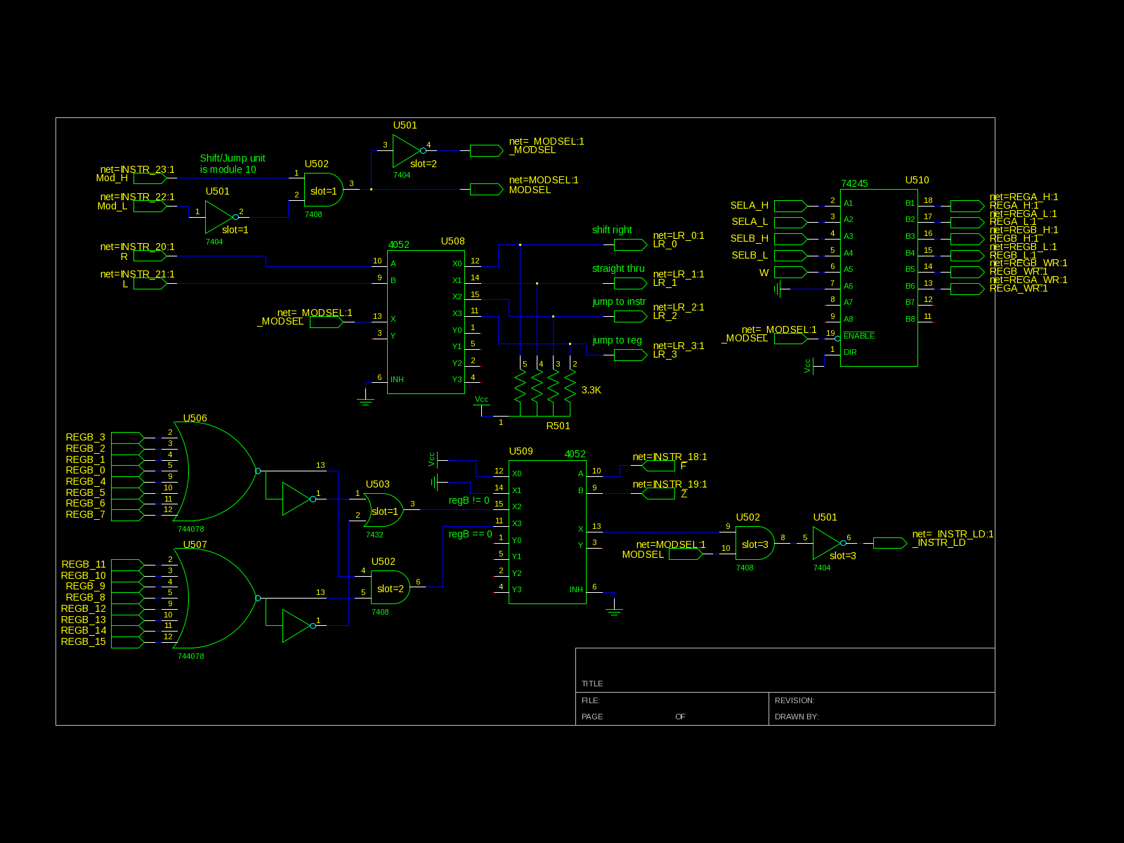
I've started working on the shift/jump unit control board.  Today I implemented the MODSEL/!MODSEL logic and the LR selectors.  For reference, here's the schematic:


Back side of board -- point-to-point wiring being used in this case.

Front of the board -- the sharpie labels will get replaced with proper printed ones when finished.

Sunday, February 13, 2011

Interface

I went ahead and soldered the headers onto the perfboard that the control bits will end up on...


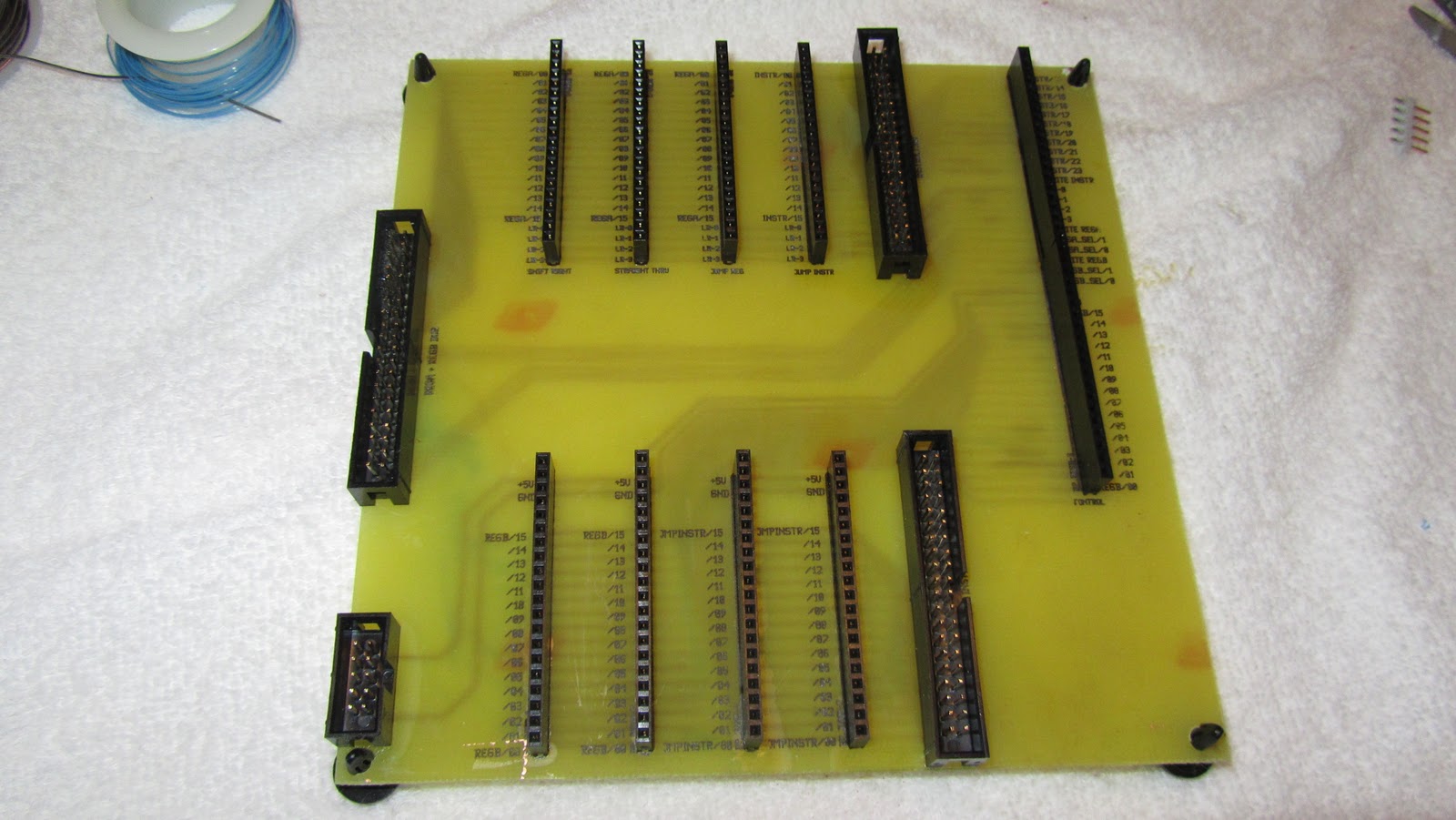
shift/jump unit backplane PCB is finished

All done: the shift/jump unit backplane is now complete.  I think it turned out pretty darn good, all things considered.

Solder-side view.  The gaggle of wires at the bottom is the
B register bus.  Since the pinout of the 40-pin socket is
such that the rightmost pin must go to the leftmost breakout,
there was no way to run the traces without using vias, which
I am not able to do.  So a little point-to-point soldering finishes it off.

Component side

I got these plastic snap-in feet from Jameco.  Must simpler than trying
to scrounge up brass standoffs and screws.

The worst section of etching on the board.  Surprisingly I only had to
re-route two of the traces.  Also notice the gummy stuff between the
pins -- I still haven't perfected my flux application, and I tend to use
too much, resulting in a gummy mess between all the pins.

I'm very happy with how the silkscreen came out.  It's surprisingly
legible, and I'm shocked it lined up as well as it does, given
that I had to align it pretty much blind.
The next steps will be building the four data transfer modules (each board will just be a pair of 74245 tristate buffers on an etched PCB), the control module (perfboard with point-to-point connections), and an A/B register bus simulator.

The A/B register bus simulator will just be a board with 32 DIP switches (16 for bus A and 16 for bus B) and a little control logic to set the outputs to hi-Z when the write signal is not asserted.  This will let me test whether the board actually works, before having actually constructed a working register file.