 |
| Back side of board -- point-to-point wiring being used in this case. |
 | |
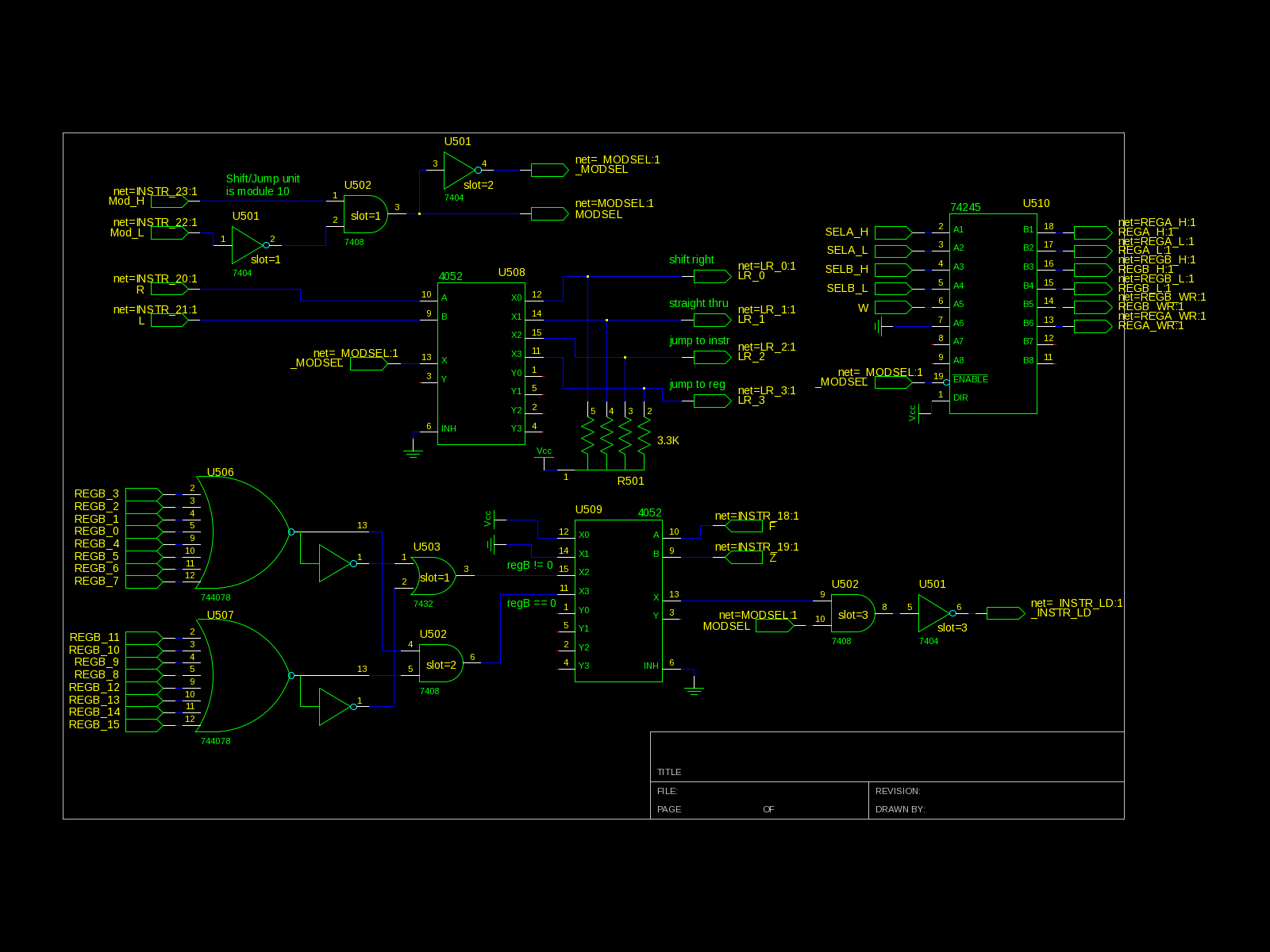
| Front of the board -- the sharpie labels will get replaced with proper printed ones when finished. |
|
| Back side of board -- point-to-point wiring being used in this case. |
| |
| Front of the board -- the sharpie labels will get replaced with proper printed ones when finished. |
 |

 |
| Solder-side view. The gaggle of wires at the bottom is the B register bus. Since the pinout of the 40-pin socket is such that the rightmost pin must go to the leftmost breakout, there was no way to run the traces without using vias, which I am not able to do. So a little point-to-point soldering finishes it off. |
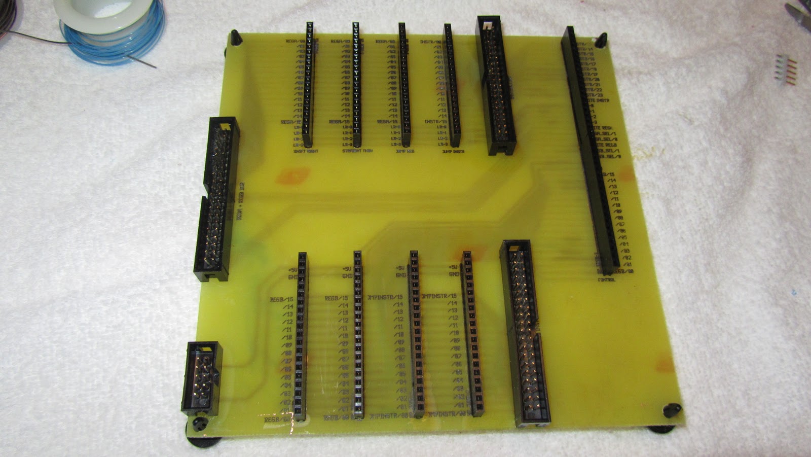 |
| Component side |
 |
| I got these plastic snap-in feet from Jameco. Must simpler than trying to scrounge up brass standoffs and screws. |
 |
| The worst section of etching on the board. Surprisingly I only had to re-route two of the traces. Also notice the gummy stuff between the pins -- I still haven't perfected my flux application, and I tend to use too much, resulting in a gummy mess between all the pins. |
 |
| I'm very happy with how the silkscreen came out. It's surprisingly legible, and I'm shocked it lined up as well as it does, given that I had to align it pretty much blind. |
