Thursday, December 30, 2010

shift/jump unit schematics

I've finished up the draft schematics for the shift/jump unit. I've split the schematics into several sheet, using common nets to link them together. I'll be laying out the PCB for this unit soon (as soon as I finish up drilling and assembly the instruction buffer PCB).

This is (most of) the control logic for the module. Notice that there isn't much complicated logic here -- the first 9 bits of the instruction are reserved for control signals:
  • bits 23 and 22: module select
  • bits 21, 20, 19, 18, 17: instruction (control signals)
  • bits 16 and 15: register bus A select
  • bits 14 and 13: register bus B select
  • bits 12-0: 13 bits of in-instruction data
The output of the modules in this sheet are expanded control signals that determine which of the following tristate buffers are enabled (thus enabling the desired function):


And this beast is a giant multiplexer that determines whether the 13-bit data region of the instruction, or the 16-bit input register, gets sent to the instruction jump bus.


One more tristate controls whether the register control signals may reach the register A/B bus:

And the last sheet simply contains the board's connectors, making it easier to draw the other schematics without having to worry about the specific pinout of the connectors.

Updated CPU architecture

As you can see above, I've modified the CPU architecture slightly after giving some further thought to the design of the register file. Notice that the "C" register bus only exists between the ALU and the register file now, whereas before it went to all modules. Also notice that the A and B register buses are now bidirectional.

My thinking with the original design was that by predefining the function of each register bus (read/write) it would make the resulting circuitry simpler in the register file. But after further consideration, I realized that the most effective and efficient way to build the register file is to have each register be its own private board, with hooks into all three register buses.

In the new design, each register will be identical in circuitry, and a DIP switch will be used to identify it to the bus. So register W will have DIPs set to 00, X to 01, Y to 10, and Z to 11. That way I can take advantage of economies of scale -- I design and build one register unit, and then simply duplicate that unit 3 more times (not too bad if I'm printing PCBs). By focusing on the design of a single register, the overall design of the register file gets much simpler, even though the individual registers are more complex (for example, tristate buffers will need to be setup to properly address the buses depending on whether that register is selected on that bus). But the upsides are many. For one, I can build one register to start, and use it to test various aspects of the other units, before the other registers are complete. Using the DIP switches, I can simulate a register behaving like any of the four registers. Finally, it simplifies the cabling between the various units, since a single 40-pin cable can now carry all of the register traffic for all but the ALU. And the ALU will have one extra link to the register file. The register file itself will be a stack of four boards, all connected in parallel on the A, B, and C register buses.

Wednesday, December 29, 2010

Willem EEPROM Programmer!

My Willem EEPROM programmer came in the mail today. As discussed in an earlier post, I was hoping to get it working by running a Windows virtual machine on my Linux PC and routing the parallel port to it. However, it appears that QEMU is not quite up to snuff when it comes to effectively simulating a real parallel port. So, I ended up tossing a second hard drive in my computer and installed Windows XP on it, then setup Grub to dual-boot. It's kludgey, but it works, and I've confirmed that the programmer interfaces just fine.

Now I just need to get some data to program, and I can run the last set of tests on the program counter before moving on to the next stage of development.

Monday, December 27, 2010

PCB design lessons learned

I've learned a few lessons after printing out my first board.
  1. Be patient! In all aspects, designing a PCB takes patience.
    • Take your time doing the toner transfer with the iron. Firm, even pressure, and at least 5 minutes under the iron.
    • When soaking the board after ironing, be patient and let the warm water disintegrate the paper, or else you risk tearing the toner off of the board.
    • When etching, don't rush -- etching a 6x6 board took me over half an hour, and as evidenced by the shorted pads, I could have probably let it etch for another few minutes.
  2. 10mil traces are OK -- but be careful! they have a tendency to smear if ground on too hard during the transfer.
  3. Touch-up before etching -- carefully inspect every trace and touch up anything that looks remotely like a gap with an etch resist pen.
  4. Invest in a circuit pen -- would have saved me a lot of time repairing traces if I could have just dabbed some conductive ink in the gap.
  5. Trust and utilize the design constraints feature of your PCB utility. Maintain at least 10mil between all components -- any closer and the error from toner smearing and/or etching errors tends to cause shorts. I think I was lucky -- I had some components as little as 5mil apart and ignored the DRC whining at me. I should have listened.
The next board I build I'll try to follow all of these rules. And of course I'll keep you posted!

Success!

Looks pretty good! I found 10 defects in the board:
  • 6 broken traces
  • 4 shorted traces
I made repairs to the broken traces by grafting in 30ga wire. The shorted traces I just hacked at with an Xacto knife until the traces broke.
I'm still waiting on my micro-drill set to arrive in the mail. Once they get here, I'll drill the holes and vias, then set to assembling the board.

PCB try #2: Success (*)

Success! (I think!)

I tried again with the transfer, this time using a glossy page cut out of a magazine, instead of the heavy photo paper. I also took more care to clean the board, and was more patient with the transfer process. Here's how the traces came out before etching:
There was 100% toner transfer -- the magazine page had white spots (bare paper) where the toner transferred off. Perfect! However, I did notice a few spots where the toner "smeared" a bit (likely due to some overzealous pressing with the iron). I touched up the pads and traces as best I could with an etch resist pen, then off to the etching. 30 minutes later, here's how it looks:
Just from the looks of it, it looks like it came out great. But close inspection of some of the 10mil traces suggests that the etchant may have come under in a few spots, creating gaps in the traces. Hence the asterisk -- I still need to go through and do a continuity test on all the pads. Hopefully the traces that are broken will be repairable by simply tinning lines with solder.

More soon...

Sunday, December 26, 2010

PCB try #1: Fail.

I went and got all the stuff I'd need to make my first PCB:
  • Some 6x6 inch single-sided copper clad boards
  • A bottle of ferric chloride
  • Samsung ML-1665 laser printer (only $39!!)
  • 50 sheets of heavy (68lb) glossy photo paper
I followed all the steps: cleaned the board, printed the traces on the photo paper, and then did the transfer with an iron. However, the resulting transfer didn't work very well:


I'm going to try again tomorrow, with a couple modifications to my process:
  • Sand the board with 600-grit paper before cleaning with alcohol and performing the transfer
  • Use the tip of the iron to grind the crap out of the traces when doing the transfer
I'm hoping that this next attempt will be more successful.

Saturday, December 25, 2010

Program counter is DONE!

Finally! The program counter is complete. This afternoon I finished soldering the remaining pins: the 24 ADDR lines going to the SIL header (that will later route into the address buffer module that I mentioned in my previous post), and the 16 ADDR_LOAD lines going from the load socket to the address counters.

I was even able to run a rudimentary test of the address loading by taking the 4th bit of the address, inverting it, and assigning that pin to the !LOAD pin of the ADDR_LOAD socket. I was then able to observe the address counting properly from 0x0007 (0111 in the last four bits) to 0x0008, saw !LOAD de-asserted, then on the next clock tick, the current address properly jumped to the value on the ADDR_LOAD socket (which happened to be 0xFFFF since the pins are tied high).

The next step for the program counter is to get an EEPROM programmer and develop a method to compile and burn code into the EEPROMs efficiently. The Willem EEPROM programmer seems to be the best bet, as it's orders of magnitude less expensive than other programmers, and its software natively supports the Atmel AT28C256 EEPROMs that I'm using. I ordered one this afternoon, and it should arrive in a couple weeks.

Of course, the Willem programmer has a couple issues:
  1. The software is Windows-only. And the software hasn't been touched sine the Win98 days, so realistically you can't go much beyond Win2000 and expect it to work.
  2. The programmer requires a parallel port. Who the heck has one of those anymore?
Surprisingly, my desktop PC (running Fedora 14) has a parallel port. Check. I created a QEMU/KVM virtual machine running Windows 2000, and added the parallel port of the host to the VM. As far as I can tell, it *should* work. But the only way to find out for sure is to go ahead and get the programmer and try it out. If all else fails, I've got enough spare hardware in my closet that I can build a Win2000 PC for the sole purpose of burning EEPROMs, but I hope it doesn't come to that.

Friday, December 24, 2010

PCB Design

I've decided to suck it up and start figuring out how to do full-on PCBs for the remaining components. Soldering the wires by hand works well enough for things like the clock unit, but my experience on the program counter has been exhausting.

After quite a bit of tinkering, I managed to persuade the gEDA Suite of open-source EDA tools to do my bidding. Today I drew up the schematics and a PCB layout for the instruction buffer unit. This unit is very simple -- it takes the 24-bit instruction as input, then routes it through a pair of 20-pin headers (for attaching the logic analyzer), then on to a set of transceivers, which will actually be driving the bus. The entire layout has only 11 components on it, but as you can see, it's a very complex design:

Now I just need to procure some photo paper, gain access to a laser printer, and then I'm off to printing my own PCB! The guides online are all the same -- it's a simple process:
  1. Print the mirror of the solder layer on heavy, glossy photo paper in a laser printer. The toner will adhere, but will transfer to the copper easily with some heat.
  2. Clean the copper board thoroughly, removing all oils and dust.
  3. Lay the print face-down on the copper, hold in place, and use an iron to heat the toner and transfer it to the copper.
  4. Soak the PCB in the chemical bath stuff to etch the copper away
  5. Rinse and clean the toner off of the traces
  6. Use a dremel or a small drill to drill the holes (drill press is appaently the best for this).
And that's it! I can't wait to give it a try and see how my first PCB turns out. I'll keep you posted here.

Sunday, December 19, 2010

Back on track!

It's been a while since I posted an update, and that's mostly because it's been a while since I've done any work on this project. But over this weekend I got back on track.

I was in the midst of a setback the last time I posted -- the program counter unit was not going well. First I found that somewhere in the myriad of connections, was a bad connection or a short, and thus the program counter quit...counting. Then, as I tried to cram the 7-segment display onto the board, I realized that I was trying to do too much with my limited resources and skills.

So this weekend I started over and got the program counter (almost) finished. Here are a few pics:


Program counter attached to the clock/reset unit

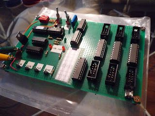
Close-up of the program counter. The four chips in the middle are synchronous 4-bit counters that provide a 16-bit address to the three Atmel EEPROMs. The EEPROMs store 8-bit words using a 15-bit address, allowing for 32k 24-bit instructions. The instructions will appear on the 24-pin header to the right.


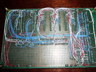
Rear of the program counter. As you can see, there are still a number of things missing. One, I still need to wire up the 24 instruction header pins to the EEPROMs. And second, the 40-pin socket that is currently unwired? That's for implementing jump instructions. So I still need to wire up the 16 "next instruction" pins to the 4-bit counters, but not until I get finished with the jump/shift unit.

What this boils down to is that I'm very close to having the ability to actually start executing some code very soon. I need to get an EEPROM programmer (I think I'll get a Willem programmer). Once I have that, I should be able to do a full system test with real code, and at least verify that I'm able to write code, compile it, burn it into the EEPROMs, and have it read out properly on the board.

After that, it's "just" a matter of getting the remaining modules done. Next up:
  1. Repeater board for the instructions. The instruction data needs to be fed to lots of different places over some very long cables. So I'll build a simple repeater board with a bunch of 8-channel buffers and 40-pin sockets and then wire it up to the program counter. The instructions will be distributed to each board using standard IDE cables.
  2. Jump/Shift unit (phase 1: basic jumps): I'll build out the basic components of the jump/shift unit, only implementing the JMP instruction (which contains the target address right in the instruction). This way I can test the jump functionality without needing the register file (which all the other jump instructions need).
  3. Register file: given the complexity, likely the first module that I'll try printing a circuit board for.
  4. Load/Store unit: needed to actually populate the register file with anything useful (and provides the system RAM)
  5. Finish the jump/shift unit
  6. ALU
  7. I/O unit
No problem, right?

Sunday, April 18, 2010

LED display progress...and problems

Today was a bit frustrating. I made some more progress on the LED display circuit, laid out here:
This circuit is designed to take the 4MHz clock coming off of the EDE707 and use it to drive a couple multiplexers and buffers (I ended up using a pair of 74LS12[56] chips instead of the 74F257). The intended waveform is shown at the top right. The CLK signal (a direct down-clock of the 4MHz) will be used to drive the LATCH pin of the EDE707. Qa will be used to select which set of inputs to use (address pins, or Qb/Qc/0/0). Qb and Qc will be used to drive the multiplexers so that the right part of the input shows up on the EDE707 inputs at the right time. Easy, right?

Here's what the program counter board looks like now:

Here's a front view with the various sockets/chips described.

So far so good, right? Well, not so much. After wiring up the 2:4 multiplexers and the quad tristates, the program counter board is now suffering from a bug such that all outputs are now held high all the time. No freaking idea why. I spent half an hour with a multimeter trying to find something resembling a short circuit, and couldn't find one.

I thought maybe it was some weird situation where a "high" output was wired to a "low" output and was thus causing a short, so I pulled all of the ICs out of the board. But even with no ICs in the board, it's still sending all of the outputs high. Which is even more bizarre, because the various output pins are isolated from each other (even more so with the ICs removed). So why would they all register +5v when the board is plugged in, even when there are no ICs in the board?

The other possibility is that my logic analyzer is no longer properly calibrated. I did notice that it said "default calibration settings loaded" the last time I booted it up.

So more research and debugging is to come. For now, however, I effectively have a paperweight that I spent a dozen hours to create. Lame.

Saturday, April 10, 2010

More progress on the program counter

Got some more wiring done today. At my last update, I had the "counter" part of the program counter done, but hadn't wired up the address pins of the EEPROMs. I've now cascaded the address pins to all three EEPROMs (32 wires, 64 solder joints) and also cascaded the address pins to a pair of 4052 dual 4:2 multiplexers. Why?
The multiplexers are part of a state machine that will be used to drive the EDE707, which I also added to the board today. The EDE707 is a pretty cool little chip -- it can drive 8x 7-seg LED displays using a microprocessor-style input. This is part of the "cool blinky lights" part of the project -- I want to have a 4-digit LED display of the current instruction. It'll be handy for debugging at slow clock speeds, and it'll look cool too!


The EDE707 runs at 4Mhz (that's the crystal sitting to the top-right of it). However, it's pretty pokey with respect to command inputs. To set the displays, you first setup a command on the four input pins (ex: 0010 for the third digit), then bounce the latch pin. Then you setup the value for that digit on the input pins, and bounce the latch pin again. Unfortunately, the datasheet says you have to leave the data active on the pins for 1.2ms (milliseconds!) after bouncing the latch. When your clock is running at 4Mhz (250ns), 1.2ms is an eternity.

The way I've decided to accommodate this is to build a simple state machine. The 4MHz clock first goes into a 12-stage ripple counter. This gets the clock pulses down to ~2ms between high-low transitions. This slower clock then goes into a 4-bit synchronous counter. The counter is used to run through a simple state machine:
  1. Counter: 0000: send 0000 (first digit) to the input pins
  2. Counter: 0001: send a0, a1, a2, a3 to the input pins
  3. Counter: 0010: send 0001 (second digit) to the input pins
  4. Counter: 0011: send a4, a5, a6, a7 to the input pins
  5. Counter: 0100: send 0010 (third digit) to the input pins
  6. Counter: 0101: send a8, a9, a10, a11 to the input pins
  7. Counter: 0110: send 0011 (fourth digit) to the input pins
  8. Counter: 0111: send a12, a13, a14, a15 to the input pins
As you can see, I can use the least-significant bit of the counter to drive a 2-input multiplexer that selects between a 4-bit piece of the address, or a command.

The commands can be driven directly from the counter -- the second and third bits are used to form the last two bits of the command.

Finally, the address information is formed by passing the address information through four 4:2 multiplexers, using the second and third bits of the counter as the selector.

When all said and done, each piece of the command takes about 2ms due to the many counter stages. Thus to get through all eight steps takes about 16ms. However, this still results in an effective polling rate of around 60Hz, which is much faster than the human eye can even perceive.

I've still got quite a bit of work to do before the program counter is done:
  1. Add the final multiplexer to drive the input pins of the EDE707
  2. Add the LED display and its driver transistors
  3. Finish wiring up the EEPROMs (I still haven't even run power and ground lines to them)
  4. Install the address load socket and wiring
  5. Install the current instruction sockets and wiring
...and then on to the shift/jump unit!

Monday, March 22, 2010

More photos

A couple more photos to show what things are looking like

Sunday, March 21, 2010

Counter is Counting...


I've reached one (of many) important milestones this evening: the program counter is now counting! It's surprising how much work it takes just to arrange four 4-bit counters and extract the resulting 16-bit address. But it's working! I've verified that the counter is able to count successfully from 0x0000 to 0xFFFF (65,536 for you decimal readers) without any missed bits or anything.

I went ahead and wired it up so that I have a 2x10-pin header that matches with my logic analyzer's termination adapters. That way it's simple to bring the ADDR signal into the analyzer as a trigger.

This accomplishment is important for a couple of reasons, because it proves a number of ideas that I will be using going forward:

  1. The buffers on the clock/control board can drive 4+ chips on an external board without any clock jitter or slew.
  2. I can pull 5V and GND through the 10-pin ribbon cableon the clock/control board without causing voltage sags or any latent current on GND.
I still have a lot of work to do on the program counter, though:
  1. Wire up the 7-segment displays and driver/decoder so that I have an address display that is always available.
  2. Wire up the ADDR LOAD pins and socket
  3. Wire up the EEPROMs and verify that 24-bit program data can be read successfully.
  4. Install two sets of buffers/line drivers for the program data
Frankly I'm not sure if I'm going to have enough real estate on the board for all this. But we'll see...stay tuned!

Wednesday, March 17, 2010

Back on track!

Hooray! I believe I've found the source of my problems. First off, there *was* a short on the board:

Notice the tin "whiskers" connecting the center pins to the pins directly to their right. Cleared those out, and I thought everything would be fine....

But it wasn't. So I pored over the whitepapers, ran Ohm's law calculations till my head started spinning, and finally went to bed really frustrated. But then I had an idea -- what if my problem isn't with the design at all? What if I was just over-driving my power supply?

My power supply is a cheapo Micronta 13.8V, 1.75A unregulated supply that I got at radio shack a zillion years ago. Could *that* be the problem?

So as an experiment, I wired up an Antec compute (regulated) power supply to the system. Bonus: computer power supplies have big fat 12v *and* 5v rails (24A on the 5v rails for my 500W supply!!). And wouldn't you know -- everything worked fine. The clock didn't get all wonky, and the program counter ticked just fine.

So next step: rip out all of my 7805s from the design and leave power generation and regulation to the power supply. I'm just going to solder in a standard Molex 4-pin power supply header to the control board, and distribute the 5V and 12V supplies like usual.

Sunday, March 14, 2010

Started on program counter

I've started working on the program counter. The sockets for the EEPROMs and the parallel load counters are all soldered in. I then prototyped the counters on my breadboard and all was well, but after soldering them up, there seems to be a short somewhere. The board is pulling almost 100mA @ 12v. To make matters worse, I blew the fuse in my multimeter while looking for the short. So...not a whole lot of progress this weekend. Once I get a new fuse, I'll keep hunting for that short. Could also be two outputs connected. Lots of pins to check. Pics of the new board to be posted soon.

Sunday, March 7, 2010

Program Counter Prototyping

I started prototyping the program counter, and ran into a bit of a jam. The 74161 synchronous counters that I ordered...looks like I inadvertently picked up the "S" version (74S161) which is rated at 80Mhz and draws a whopping 475mW at 5V. With four of them (for 16 bits) in parallel, I measured 2 ohms across the power leads:

V/R=I

5/2 = 2.5A

Yikes! My little 1A 7805 simply can't drive them. What I *wanted* was the 74LS161, which is rated at "only" 30Mhz, but uses a reasonable 35mW at full load.

I'm also considering running an unregulated 12V rail to each sub-board, so that if a sub-board needs more power than can be provided by the clock/control unit, a 12V rail is available for a 7805 to bolster the power capacity.

Clock/Control unit is DONE!

All done! The clock unit is assembled:

Now on to the program counter...

Saturday, March 6, 2010

More bus transceiver work

I managed to get the majority of the wiring for the bus transceivers done today. Check out this bundle:

The first two plugs are wired up; I should be able to get the other four done this weekend. Then the clock/control unit will finally be complete!!

Friday, March 5, 2010

Demonstrating a Schmitt Trigger

In my last batch of parts from Jameco, I also picked up a hex Schmitt Trigger. Schmitt triggers are nice because they don't suffer from the bouncing effects of a normal inverter. The input signal must drop below a certain threshold for the output to go high, and it must go above a different threshold for the output to go low. I did some traces on my analyzer to demonstrate the difference.

The circuit involved looks like this:


The RC circuit gives a slow rise from 0 to 5v when power is first applied. That input goes into an inverter, so that the RST signal goes low some short time after power up. The OR gate collects the RC circuit and the RST toggle switch into a single signal. The debouncer cleans up the mess that the (non-Schmitt Trigger) inverter makes of the RC signal, and the D-flip-flop ensures that the RST signal only changes on the falling clock edge (and conveniently provides a !RST signal too).

Here's what the timing run looks like with a normal inverter:

Notice that the output of the initial inverter bounces for over 12ms as the voltage rises. The debouncer removes the jitter and provides a clean edge to the signal, which is picked up on the flip-flop output at the next falling clock edge (not shown).

Now here's the same trace, but I've replaced the inverter on my board with the Schmitt Trigger:

No bouncing! So if I'd used a Schmitt Trigger in the first place, I could have avoided the debouncing step, right?

Not really. The clock circuit I'm using depends on an inverter that behaves in a somewhat analog fashion. With the Schmitt Trigger in there, the clock doesn't tick properly. So rather than have a whole separate IC on the board just for power-on-reset debouncing, I just utilized a few more channels from the debouncing chip (which was already on the board anyway for the toggle switches).

Bus transceivers

I've started installing the bus transceivers for the clock/control module. There will be six other boards to control, so I'm putting in six 10-pin shrouded sockets. Each socket will provide two 5V lines, 2 GND lines, CLK, !CLK, RST, and !RST. Each of the non-power signals will be driven by one channel of a 74HCT245 transceiver chip. These transceivers are designed to drive up to 15 TTL chips per channel.


As you can see from the backside of the board, I'm not quite finished with the wiring yet. I've only wired up the "head" transceiver, which itself will drive the three "sub" transceivers.

Monday, March 1, 2010

Open-source Logic Analyzer

My friend over at neodux.com pointed me to this link at hackaday for a $45 open-source logic analyzer. Pretty cool stuff. 32 channels @ 100Mhz. You can get similar functionality from something like a USBee, but those are closer to $100. I got my monstrous HP analyzer for $100 on Craigslist. So $50 or so for the open-source one is still a great deal!

Logic Analyzer Cart

My logic analyzer came with a pretty nice steel cart. It had big casters so it slid over the carpet easily, built-in storage, and fit the analyzer just right. Only problem -- the damn thing was wider than my closet doorway! Logic analyzers are useful, but they're sure not "pretty". My wife and I got a bit tired of the analyzer sitting in our office instead of it being in the closet where it belonged. So I whipped up a new cart for it this weekend. The new one has more storage than the old one, which is good. Only downside is that since the casters are directly under the corners of the analyzer, it's a bit unstable when pushed around. I have to be careful to not push it around too fast or it's liable to fall over. The old cart was wide for a reason: so you didn't have to worry about such things. Some test rolls with the new cart show that it's indeed mobile, however. And it fits in the closet. Which was really the point all along.

Tuesday, February 23, 2010

System Architecture

Drew up the system architecture. The modules (gray units) are individually selected by the first two bits of the instruction. That way I can isolate each board for different types of instructions. Each board will have five bits of "instruction" to work with. The wide buses will be implemented using 40-pin rounded IDE cables (32 bits + 8 bits of control) .

The register file is where everything happens -- all of the instruction-processing units select one or two registers to read, the contents of which will be presented on the "blue" bus. They can also select a third register to write -- this can be the one of the registers being read. Registers/RAM are written on the rising clock edge.

The program counter presents the current instruction to all of the processing modules. It has a single feedback link to the jump/shift unit, which is capable of writing a new 15-bit address into the counting register. The program counter commits data and presents a new instruction on the falling clock edge.

Sunday, February 21, 2010

Program Counter plans

Drew up the program counter plans in gschem. Again, the final results are tidy and nice-looking, but I don't like how gschem restricts you to a tiny box within which to put all the components...

Saturday, February 20, 2010

Control Unit is done!

Finished up the control unit today. All that is left is to add the transceivers and six connectors that will carry the clock, power, and reset signals to the other boards. Here's my workspace:


Notice the logic analyzer -- very handy for verifying expected clock frequencies as well as the effectiveness of the debouncing and synchronization latches for the power-on-reset circuitry.

...and the backside of the finished board. The empty side will be populated with the transceivers and shrouded connectors as soon as they arrive in the mail. This is my first time soldering a perf board like this since college...so I'm still a little rusty.


Front side of the finished board. Definitely much tidier. The DIP switches at the top left are the clock frequency selectors. The legend is on the chart at the bottom right. The CLK toggle at the top is for manipulating the clock signal when in manual clock mode. The RST toggle is self-explanatory, except to note that the signal runs through a debouncer and a D-latch to ensure that you always come out of reset on the falling edge of the clock.


Chips used:
  • 7805 5V regulator
  • EDE2008 debouncer
  • 4020 14-stage binary counter
  • 4069 hex inverter (1/2 used)
  • 4051 3:8 single channel multiplexer
  • 4013 dual D flip flop (1/2 used)
  • 7432 quad 2-input OR gate (1/4 used)

Friday, February 19, 2010

Better schematic


The clock unit was the first schematic I drew up. They got much better looking as I went on. For example, this is the load/store unit...

Electronic or Paper?


I tried using gschem today to draw up the program counter circuit, which I had already drawn up on paper. I found laying out the circuit in an EDA tool cold and unforgiving. Paper was much more satisfying. What do you think? I'm thinking I'll stick with paper, especially given that I've already completed all the plans on good ol' graph paper...

New Blog

I've decided to go ahead and create a blog to document my progress on building my homebrew CPU. It's not going to be an easy project. It's not going to be a short project. But I do expect it to be pretty fun. Believe it or not, I'm in pretty good company when it comes to building homebrew CPUs:

  • BMOW - Big Mess O' Wires - this is the first homebrew CPU I'd ever seen. The designer is a lot like me -- not an electrical engineer, just a hobbyist. He built a very impressive working computer using wire-wrap sockets. Wow.
  • MyCPU - Another very impressive project. This guy is definitely on the "high end" of homebrew design, complete with a passive backplane and replaceable cards in his design. Oh, and custom printed PCBs!! He's even published all of his work so you can build one yourself (which many have done). His homebrew CPU is even network-connected, runs Minix, and hosts his webserver. Wow.
  • HomebrewCPU - I stumbled upon this one when creating this blog -- I wanted to use homebrewcpu.blogspot.com but it was taken. Haven't read much into this guy's blog, but he looks to be doing about the same thing I want to do.
  • Props to my friend Sean for sending me this link...
So just what is it that I am trying to do?

Project Goals:
  • HAVE FUN! Any of the rules may be broken if following them starts to feel more like drudgery than a fun project.
  • Design a functional, programmable CPU that is capable of doing useful things, like playing Tetris, Pong, or maybe even a custom OS.
  • The design will all be done using (effectively) pencil and paper. Not because there isn't automation software available (see here), but because there's something visceral and interesting about getting down to basics.
  • NO MICROCONTROLLERS! I would feel like that's totally cheating. The design will be comprised of mostly 4700 and 4000-series logic, with more complex circuits for things like the ROM and RAM. Pre-programmed microcontrollers like the EDE707 I'll use for non-essential stuff like driving LED displays.
  • KISS - gotta keep it simple, since I'm not an EE and won't be able to debug really hairy stuff.
  • No custom PCBs. Too much work, feels like cheating since I don't have to solder anything but the pins. Automatic place and route takes all the satisfaction out of completing a complex build.
  • No microcode. Sound impossible? It's not. In fact, I've already finished my instruction set and have figured out how to design the CPU to work without a single microcode unit. The most complex "microcode" will be a few (as in 1-2 per board) AND and OR gates.
  • It's gotta look cool. Lots of blinky LEDs and 7-segment displays so that you can "see" the CPU functioning.
Target System Architecture

After a fair amount of research, I've determined that this will be an optimal architecture for my design. Again, I'm in good company -- this is how most other homebrew CPU designers setup their systems.
  • 16-bit registers and ALU
  • 24-bit fixed-width instructions
  • Harvard architecture design (as opposed to a von Neumann architecture)
  • Single-cycle operation. This requires more chips (everything has to be parallel) but is much easier to design and debug.
Build Strategy

This is a big project, so I need to make sure that I'm able to build it in discrete chunks, each of which plug into the larger architecture and work largely independent of each other. I've designed seven major components, that I plan to build in this order:
  1. Control Unit - Power, reset, and clock signals for the whole design
  2. Program Counter - EEPROM unit and 16-bit loadable address register
  3. Register File - 4x 16-bit registers with 2 reads and 1 write to any of the four
  4. Jump/Shift Unit
  5. Arithmetic Logic Unit - 16-bit parallel ALU based on the 74181 chip
  6. Load/Store Unit - 512K RAM in 16-bit words
  7. I/O unit - graphical LCD display and keyboard input
So here we go!

So that's it -- a quick summary of the design. As we speak I already have the schematics done, the instruction set figured out, and I'm about halfway through building the control unit. I'll be posting pictures, progress, etc. as I get more time.