All done: the shift/jump unit backplane is now complete. I think it turned out pretty darn good, all things considered.
 |
| Solder-side view. The gaggle of wires at the bottom is the B register bus. Since the pinout of the 40-pin socket is such that the rightmost pin must go to the leftmost breakout, there was no way to run the traces without using vias, which I am not able to do. So a little point-to-point soldering finishes it off. |
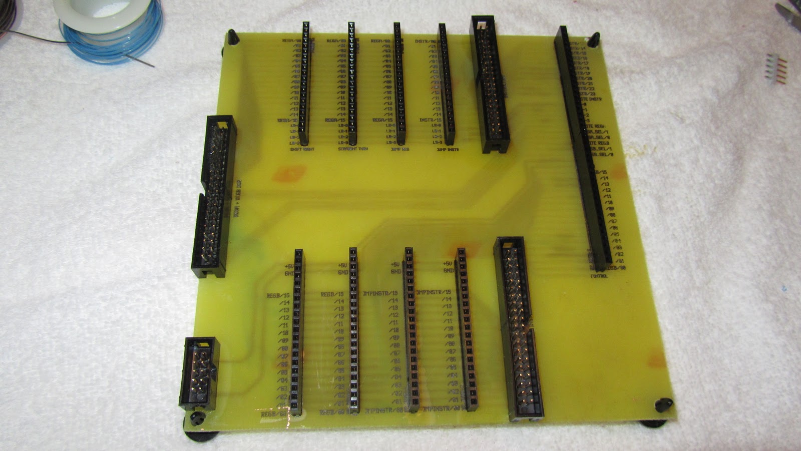 |
| Component side |
 |
| I got these plastic snap-in feet from Jameco. Must simpler than trying to scrounge up brass standoffs and screws. |
 |
| The worst section of etching on the board. Surprisingly I only had to re-route two of the traces. Also notice the gummy stuff between the pins -- I still haven't perfected my flux application, and I tend to use too much, resulting in a gummy mess between all the pins. |
 |
| I'm very happy with how the silkscreen came out. It's surprisingly legible, and I'm shocked it lined up as well as it does, given that I had to align it pretty much blind. |
The A/B register bus simulator will just be a board with 32 DIP switches (16 for bus A and 16 for bus B) and a little control logic to set the outputs to hi-Z when the write signal is not asserted. This will let me test whether the board actually works, before having actually constructed a working register file.

To remove flux I use an old tooth brush and lots of acetone, after a couple of seconds of scrubbing and it's gone. Rinse with water and dry.
ReplyDeleteGreat tip! I'll give that a try.
ReplyDelete